Si/CdTe Compton Camera
Over the past 15 years, we have been working on the next generation gamma-ray detector, “Si/CdTe semiconductor Compton camera,” with the aim of high-sensitivity observations for gamma-ray astronomy.
Semiconductor imaging detectors are desired for Compton imaging. The energy and position resolution provided with semiconductors should improve the angular resolution and hence the sensitivity of Compton cameras. From this perspective, several semiconductor-based Compton cameras have been proposed. However, most of these cameras have been developed based on combining a semiconductor such as silicon with scintillators. Taking advantage of significant progress, we have performed in CdTe technology, we have been developing a new generation of Compton telescope (e.g. Takahashi et al. 2001,2002,2004; Watanabe et al. 2005; Takeda et al. 2008) , the semiconductor Compton telescope by combining Si and CdTe, as the Si/CdTe semiconductor Compton camera.
Press Release (2012 March 29)
-
Visualization of Radioactive Substances
with JAXA's 'Ultra-wide-angle Compton Camera' - Attachment-1
- Attachment-2
Dust containing radioactive materials dispersed following the Fukushima nuclear power plant accident in March 2011. Gamma-rays are emitted in the process when unstable nuclei in the materials decay. Based on our technology of the Si/CdTe Compton Camera, we have manufactured a quick prototype model for the use in the field. The camera, now called an ``Ultra-Wide-Angle Compton Camera'' was successfully applied to visualize the distribution of radio-active substances in the Fukushima area
Presentations
- A portable Si/CdTe Compton camera for visualizing radioactive substances
- (IEEE, Nucl. Sci. Symposium, Seoul, Korea, 2013)
View Graph - To uncover hotspots of radiation with a Si/CdTe Compton Camera
- (HSTD9 - International "Hiroshima" Symposium on the Development and Application of Semiconductor Tracking Detectors, Hiroshima, 2013)
View Graph - Visualization of Radioactive Substances with
a Si/CdTe Compton Camera
- ( IEEE, Nucl. Sci. Symposium, Anaheim, 2012 ) Proceedings
- High Resolution CdTe detectors and Applications to Gamma-ray Imaging
- (IEEE, Nucl. Sci. Symposium, Valencia, 2011) View Graph
- High Energy and Position Resolution CdTe Diode Double-Sided Strip Detectors
- (IEEE, Nucl. Sci. Symposium, Valencia, 2011) View Graph
- in-vivo multi-probe tracker based on astrophysical gamma-ray detector technology
- (IEEE, Nucl. Sci. Symposium, Valencia, 2011) View Graph
- Recent Advances on CdTe/CdZnTe detectors
- (International Conference on New Developments In Photodetection,NDIP08, 2008) View Graph
- See also
- High Resolution CdTe detectors
Compton scattering typically plays a dominant role in the energy band from a few keV s to 10 MeV. It entails elastic collision between an incident photon and an electron in the scattering medium. In conventional Compton cameras, the incident gamma-ray is identified by successive interactions in two detector layers. The ideal case would be that a gamma-ray photon emitted from the source is Compton-scattered in the first layer and then photo-absorbed in the second layer. Once the locations and energy deposites of both interactions are measured, Compton kinematics allows us to calculate the energy and direction (as a cone in the sky) of the incident gamma-ray
For every event, a cone can be reconstructed as an opening angle. The source is somewhere on the cone surface. Compton cameras offer the advantage of needing only small number of photons to recover the position of sources without mechanical collimators in front of the camera. If the direction of a recoil electron can be measured, the Compton cone is reduced to a segment of the cone, the length of which depends on recoil electron measurement accuracy.
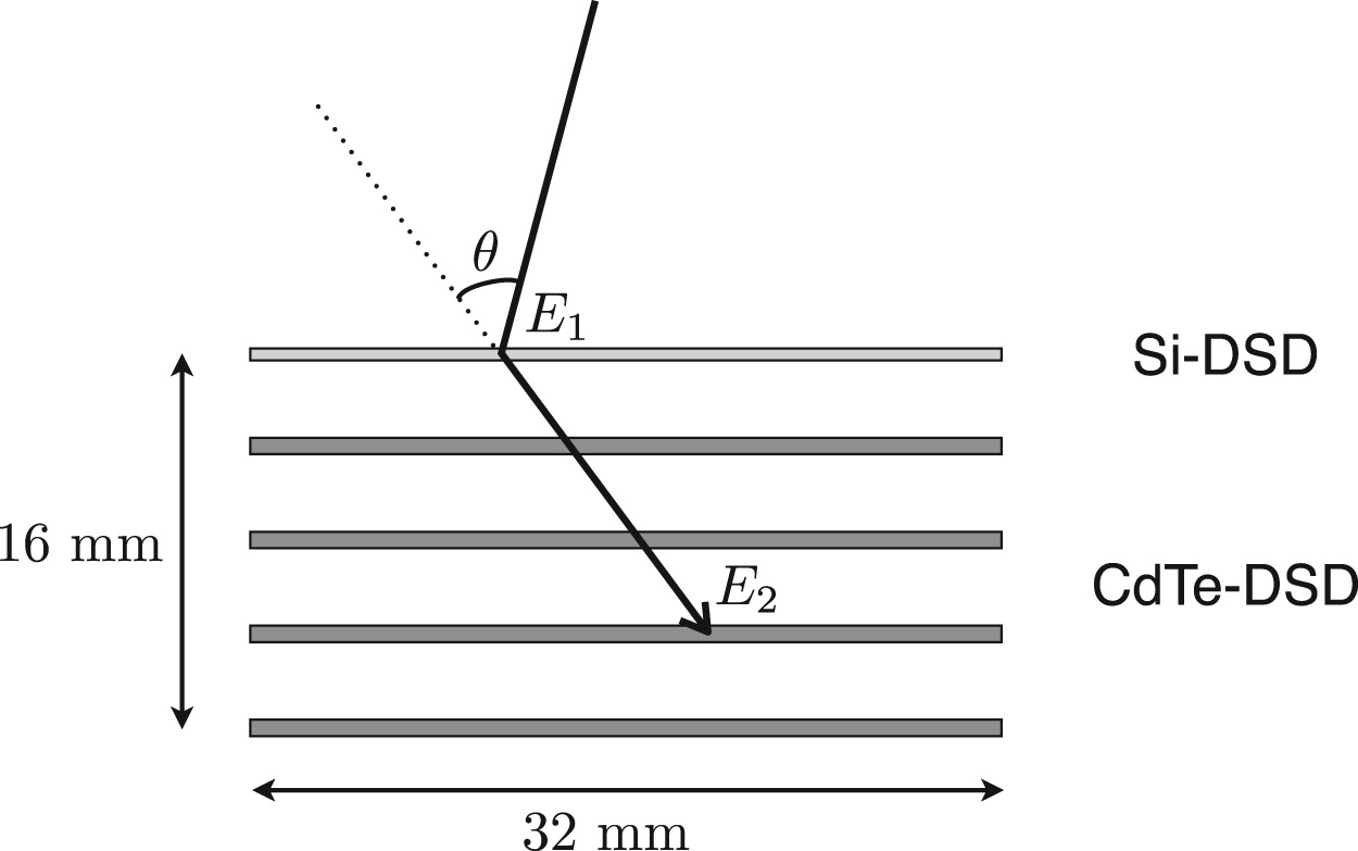
Fig. 1
Schematic drawing of the Si/CdTe Compton camera.
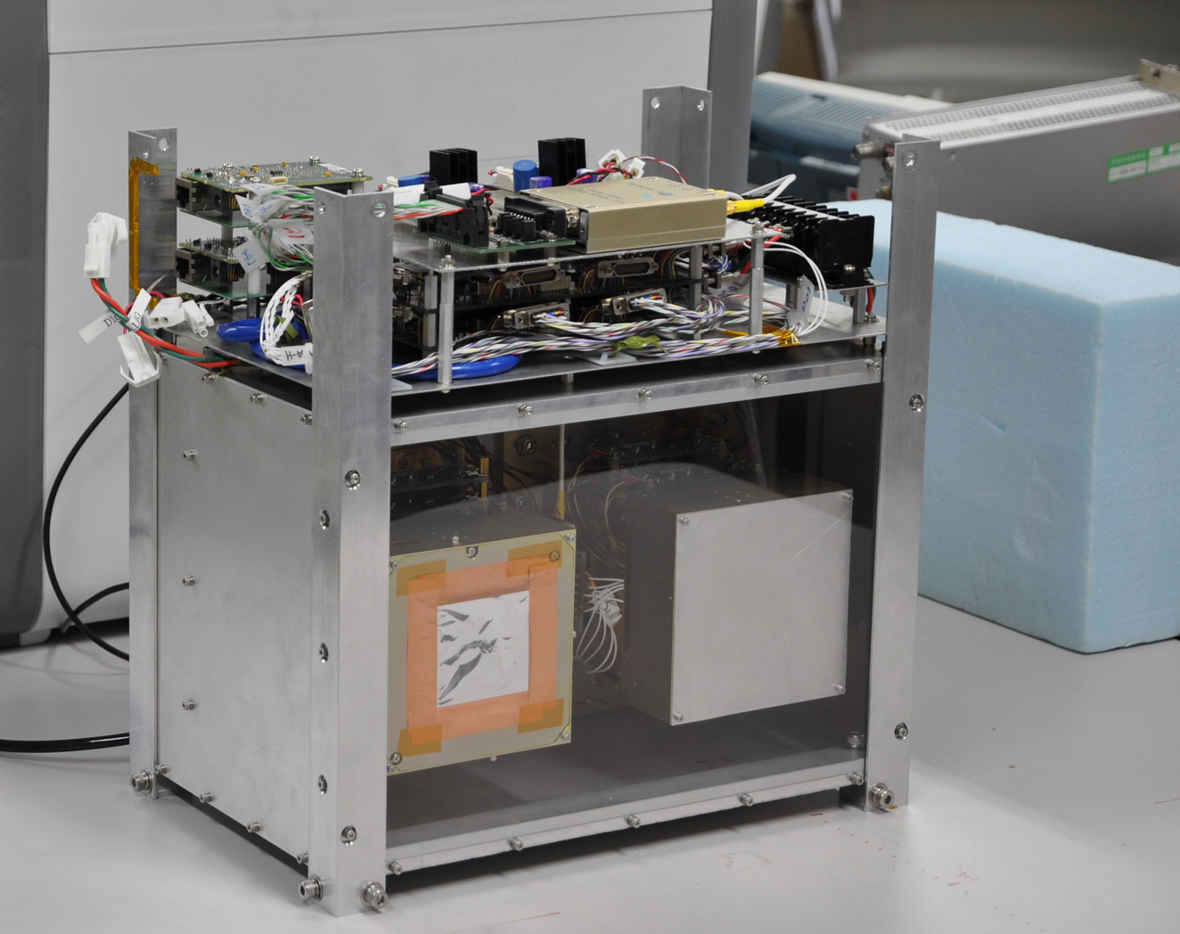
Fig 2
Si/CdTe Semiconductor Compton Camera BBM (2007)
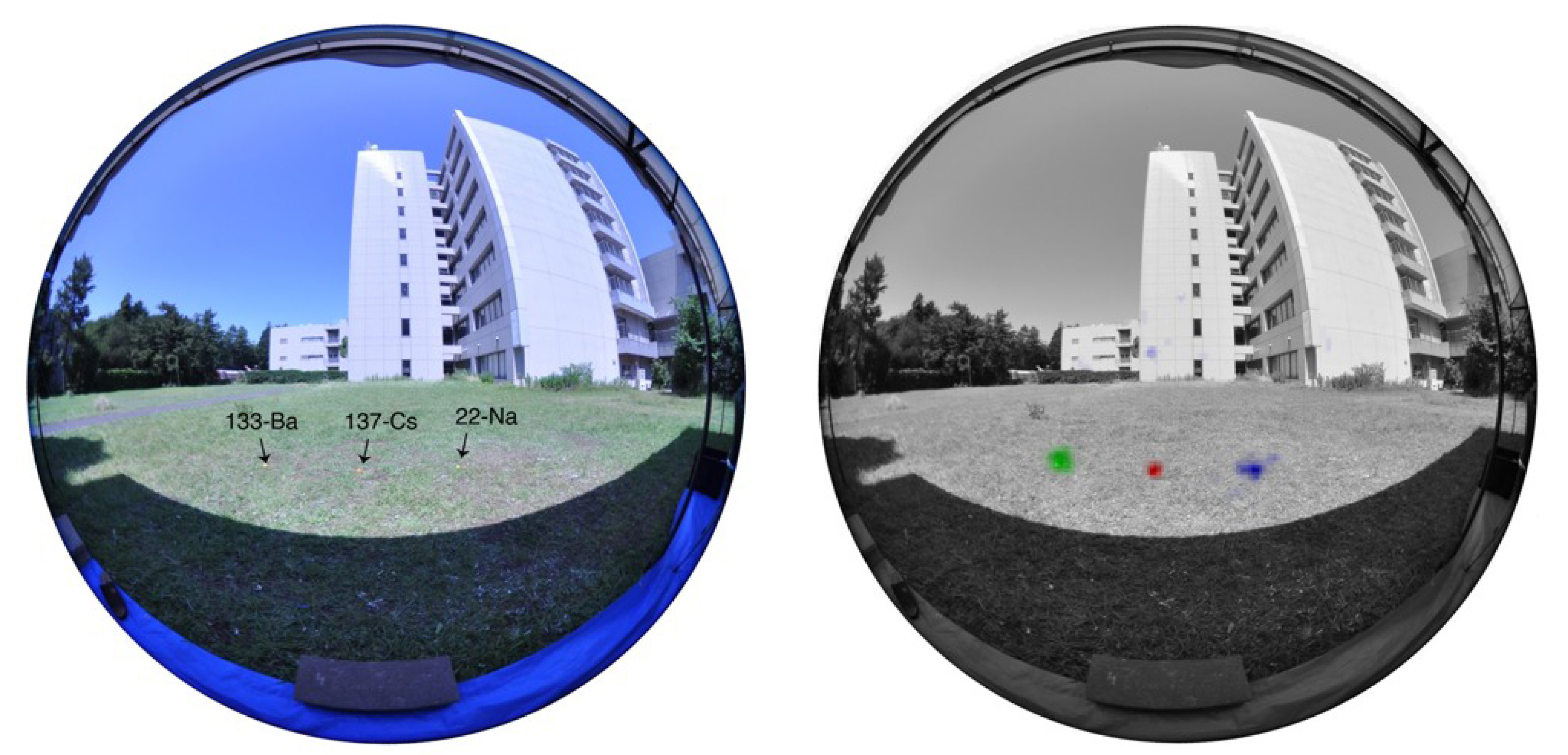
Fig. 3
(Left) Optical picture taken by a digital camera with a circular fisheye lens. The
133Ba,
22Na and
137Cs point sources are located on the
ground. (Right) Gamma-ray image combined with the optical picture. (Takeda et al. 2012)
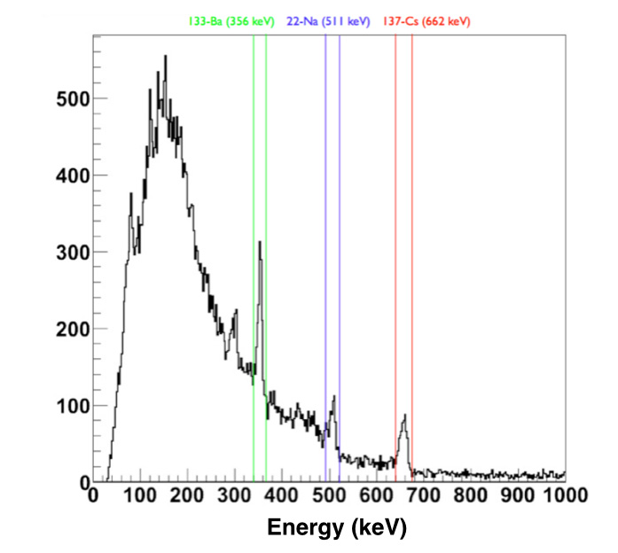
Fig. 4
Energy spectrum obtained by the imaging test with the energy windows for each gamma-ray line
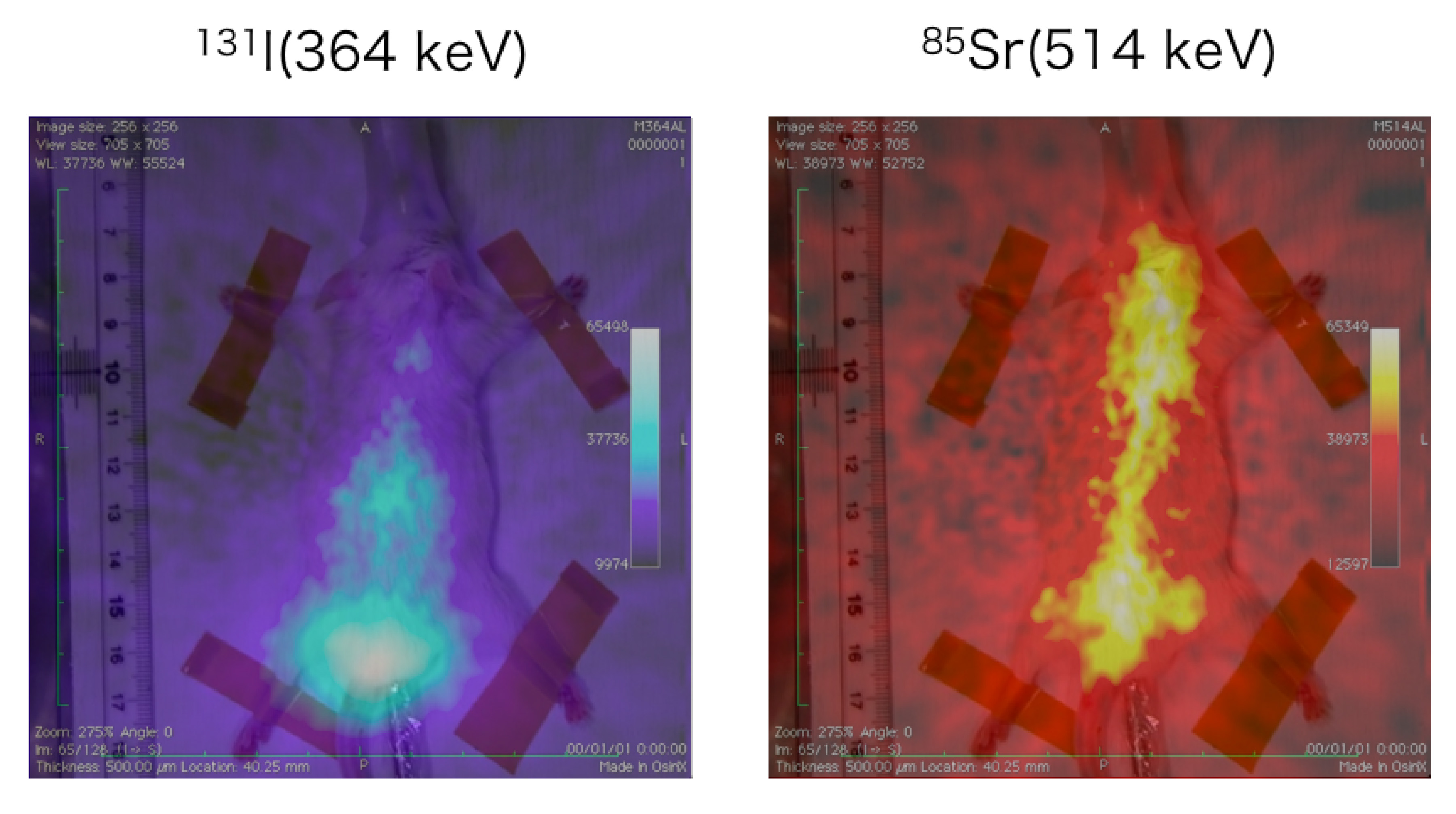
Fig. 5
The accumulation of iodinated (I-131) methylnorcholestenol (left) and Sr-85 (right) with a picture of the subject mouse
(length of about 7 cm) (Takeda et al. 2012)
In the Si/CdTe Compton camera, events involving the incident gamma-ray being scattered in the Si detector and fully absorbed in the CdTe detectors are used for Compton imaging. The direction of the gamma-ray is calculated by solving the Compton kinematics with information concerning deposit energies and interaction positions recorded in the detectors. In principle, each layer could act not only as a scattering part but also as an absorber part. Since CdTe has large atomic numbers (48, 52) and high density (5.8 g/cm3), it offers the potential to replace scintillators and to form a full-semiconductor Compton camera.
A very compact, high-angular resolution (fineness of image) camera could be realized if we were able to fabricate successfully semiconductor imaging elements made of Si and CdTe, which have excellent performance in position resolution, high-energy resolution, and high-temporal resolution. The field of view of the camera is determined from the gap between each layers, because events coming from large angle with resect to the detector plane, if we can cover the large angle scattering.
The effect of the doppler broadening, which degrades the angular resolution of the imaging system, is smaller in the Si devices than other semiconductor devices, allowing the difference between the measured and actual scattering angles to be constrained. The effect of the Doppler broadening becomes smaller as the incident energy becomes higher, because the binding energy and momentum of electrons in materials become relatively small for gamma-ray photons with higher energies.
Papers
2016
2015
2014
2013
-
The Si/CdTe semiconductor Compton camera of the ASTRO-H Soft Gamma-ray Detector (SGD)(
- ( Shin Watanabe, Hiroyasu Tajimac, Yasushi Fukazawa, Yuto Ichinohe, Shin’ichiro Takeda, Teruaki Enoto, Taro Fukuyama, Shunya Furui, Kei Genba, Kouichi Hagino, Atsushi Harayama, Yoshikatsu Kuroda, Daisuke Matsuura, Ryo Nakamura, Kazuhiro Nakazawa, Hirofumi Noda, Hirokazu Odaka, Masayuki Ohta, Mitsunobu Onishi, Shinya Saito, Goro Sato, Tamotsu Sato, Tadayuki Takahashi, Takaaki Tanaka, Atsushi Togo, Shinji Tomizuka Nucl. Instr. Method (2014): ) [PDF 1.6 MB] )
- Three-Dimensional and Multi-Energy γ-ray Simultaneous Imaging Using a Si/CdTe Compton Camera
- ( Yoshiyuki Suzuki, Mitsutaka Yamaguchi, Hirokazu Odaka, Hirofumi Shimada, Yukari Yoshida,Kota Torikai, Takahiro Satoh, Kazuo Arakawa, Naoki Kawachi, Shigeki Watanabe, Shin'ichiro Takeda, Shin-nosuke Ishikawa, Hiroyuki Aono, Shin Watanabe, Tadayuki Takahashi and Takashi Nakano, Radiology 267.3 (2013): 941-947. )
2012
- Visualization of Radioactive Substances with a Si/CdTe Compton Camera
- ( Tadayuki Takahashi, Shin'ichiro Takeda Shin Watanabe, and Hiroyasu Tajima IEEE Transaction on Nuclear Science (Conference Record, Anaheim, 2012) [PDF 5.1 MB] )
-
Applications and imaging techniques of a Si/CdTe Compton gamma-ray camera
- (
Shin'ichiro Takeda, Yuto Ichinohe, Kouichi Hagino, Hirokazu Odaka, Takayuki Yuasa, Shin-nosuke Ishikawa, Taro Fukuyama, Shinya Saito, Tamotsu Sato, Goro Sato, Shin Watanaba, Motohide Kokubun, Tadayuki Takahashi, Mitsutaka Yamaguchi, Hiroyasu Tajima, Takaaki Tanaka, Kazuhiro Nakazawa, Yasushi Fukazawa, Takashi Nakano,
Physics Procedia Volume 37,2012, pp. 859-866
(TIPP 2011 - Technology and Instrumentation in Particle Physics 2011) >[PDF 1.3 MB] ) -
Demonstration of in-vivo Multi-Probe Tracker Based on a Si/CdTe Semiconductor Compton Camera
- ( Shin’ichiro Takeda, Hirokazu Odaka, Shin-nosuke Ishikawa, Shin Watanabe Hiroyuki Aono, Tadayuki Takahashi, Yousuke Kanayama, Makoto Hiromura and Shuichi Enomoto, IEEE Transaction on Nuclear Science vol.59 No.1 p.70-76 (2012) [PDF 1.3 MB] )
2011
- High-Resolution CdTe Detectors and Application to Gamma-Ray Imaging
- ( T. Takahashi, S. Watanabe, S. Ishikawa, S. Takeda, G. Sato, Biological and Medical Sensor Technologies, Ed. K. Iniewski, CRC Press, 2011 )
- High-resolution Compton cameras based on Si/CdTe double-sided strip detectors
- ( Hirokazu Odaka, Yuto Ichinohe, Shin'ichiro Takeda, Taro Fukuyama, Koichi Hagino, Shinya Saito, Tamotsu Sato, Goro Sato, Shin Watanabe, Motohide Kokubun, Tadayuki Takahashi, Mitsutaka Yamaguch, Takaaki Tanaka, Hiroyasu Tajima, Kazuhiro Nakazawa, Yasushi Fukazawa, Nucl. Instr. and Method, A in press. (2011) )
2010
- High-Resolution CdTe Detectors and Application to Gamma-Ray Imaging
- ( T. Takahashi, S. Watanabe, S. Ishikawa, Semiconductor Radiation Detection System, Ed. K. Iniewski, CRC Press, pp.171-192, 2010 )
- Polarimetric performance of Si/CdTe semiconductor Compton camera
- ( S. Takeda, H. Odaka, J. Katuta, S,-N, Ishiawa, S.-I, Sugimoto, Y. Koseki, S. Watanabe, G. Sato, M. Kokubun, T. Takahashi, K. Nakazawa, Y. Fukazawa, H. Tajima, H. Toyokawa, NIM A, 622, pp. 619-627, (2010) )
2008
- Experimental results of the gamma-ray imaging capability with a Si/CdTe semiconductor Compton camera,"
- ( S. Takeda, H. Aono, S. Okuyama, S. Ishikawa, H. Odaka, S. Watanabe, M. Kokubun, T. Takahashi, K. Nakazawa, H. Tajima, N. Kawachi IEEE Trans. Nucl. Sci., 56, 3, PP. 783 - 790 [PDF 3.9 MB] )
2007
- New CdTe pixel gamma-ray detector with pixelated Al schottky anodes
- ( Watanabe, S., Ishikawa, S., Takeda, S., Odaka, H., Tanaka, T., Takahashi, T., Nakazawa, K., Yamazato, M., Higa, A., Kaneku, S. JJAP, 46, pp. 6043-6045, 2007 )
- Development of Double-Sided Silicon Strip Detectors (DSSD) for a Compton Telescope
- ( S. Takeda, S. Watanabe, T. Tanaka, K. Nakazawa, T. Takahashi, Y. Fukazawa, H. Yasuda, H. Tajima, Y. Kuroda, M. Onishi, K. Genba, NIM A, 579, pp. 859-865,2007 )
- Development of Semiconductor Imaging Detectors for a Si/CdTe Compton Camera
- ( S. Watanabe, S. Takeda, S.N. Ishikawa, H. Odaka, M. Ushio, T. Tanaka, K. Nakazawa, T. Takahashi, H. Tajima, Y. Fukazawa, Y. Kuroda, M. Onishi NIM A, 579, pp. 871-877,2007 )
- Performance Study of Si/CdTe Semiconductor Compton Telescopes With Monte Carlo Simulation
- ( H. Odaka, S. Takeda, S. Watanabe, S.N. Ishikawa, M. Ushio, T. Tanaka, K. Nakazawa, T. Takahashi , H. Tajima, Y. Fukazawa,. NIM A, 579, pp. 878-885,2007 )
2006
- A Si/CdTe Compton Camera for gamma-ray lens experiment
- ( Tadayuki Takahash, Experimental Astronomy, Volume 20, pp. 317-331, 2006) [PDF 1.4 MB]
- Recent results from a Si/CdTe semiconductor Compton telescope
- ( Takaaki Tanaka, Shin Watanabe, Shinichiro Takeda, Kousuke Oonuki, Takefumi Mitani, Kazuhiro Nakazawa, Takeshi Takashima, Tadayuki Takahashi, Hiroyasu Tajima, Naoyuki Sawamoto, Yasushi Fukazawa, Masaharu Nomachi, NIM A, NIM A, 568, pp. 375-381, 2005)
- Development of CdTe Pixel Detectors for Compton Cameras
- ( Shin Watanabe , Takaaki Tanaka , Kousuke Oonuki , Takefumi Mitani , Shin'ichiro Takeda , Tetsuichi Kishishita , Kazuhiro Nakazawa , Tadayuki Takahashi , Yoshikatsu Kuroda, Mitsunobu Onishi, Nucl. Instr. Meth. A, 567, pp. 150-153, 2006 )
- Recent results from a Si/CdTe semiconductor Compton telescope
- ( Takaaki Tanaka, Shin Watanabe, Shinichiro Takeda, Kousuke Oonuki, Takefumi Mitani, Kazuhiro Nakazawa, Takeshi Takashima, Tadayuki Takahashi, Hiroyasu Tajima, Naoyuki Sawamoto, Yasushi Fukazawa, Masaharu Nomachi, NIM A, vol.568 p.375-381, 2006 )
- Development of CdTe Pixel Detectors for Compton Cameras
- ( Shin Watanabe, Takaaki Tanaka, Kousuke Oonuki, Takefumi Mitani, Shin'ichiro Takeda, Tetsuichi Kishishita, Kazuhiro Nakazawa, Tadayuki Takahashi, Yoshikatsu Kuroda, Mitsunobu Onishi, Nucl. Instr. Meth. A, 567, pp.150-153、2006 )
2005
- Results of a Si/CdTe Compton telescope,
- (Kousuke Oonuki, Takaaki Tanaka, Shin Watanabe, Shin'ichiro Takeda, Kazuhiro Nakazawa, Takefumi Mitani, Tadayuki Takahashi, Hiroyasu Tajima, Yasushi Fukazawa, Masaharu Nomachi, HIGH-ENERGY DETECTORS IN ASTRONOMY, SPIE, vol. 5922, pp. 78-88, 2005 [PDF 1.8 MB] )
- A Si/CdTe Semiconductor Compton Camera
- (Shin Watanabe, Takaaki Tanaka, Kazuhiro Nakazawa, Takefumi Mitani, Kousuke Oonuki, Tadayuki Takahashi, Takeshi Takashima, Hiroyasu Tajima, Yasushi Fukazawa, Masaharu Nomachi, Shin Kubo, Mitsunobu Onishi, Yoshikatsu Kuroda, IEEE Trans. Nucl. Sci., pp.2045-2051, 2005. [PDF 3.1 MB] )
2004
- Application of CdTe for the NeXT Mission
- (Tadayuki Takahashi, Kazuhiro Nakazawa, Shin Watanabe, Goro Sato, Takefumi Mitani, Takaaki Tanaka, Kousuke Oonuki, Ken'ichi Tamura, Hiroyasu Tajima, Tuneyoshi Kamae, Greg Madejski, Masaharu Nomachi, Yasushi Fukazawa, Kazuo Makishima, Motohide Kokubun, Yukikatsu Terada, Jun Kataoka, Makoto Tashiro, Nucl. Instr. Meth. A, in press, 2004 [PDF 2.3 MB] )
- Development of a Si/CdTe semiconductor Compton telescope
- (Takaaki Tanaka,Takefumi Mitani,Shin Watanabe,Kazuhiro Nakazawa, Kousuke Oonuki, Goro Sato, Tadayuki Takahashi, Ken'ichi Tamura, Hiroyasu Tajima, Hidehito Nakamura, Masaharu Nomachi, Tatsuya Nakamoto, Yasushi Fukazawa Proc. SPIE, vol. 5501, 229-240, 2004 [PDF 1.5 MB] )
- Wide band X-ray Imager (WXI) and Soft Gamma-ray Detector (SGD) for the NeXT Mission
- (T. Takahashi, A. Awaki, T. Dotani, Y. Fukazawa, K. Hayashida, T. Kamae, J. Kataoka, N. Kawai, S. Kitamoto, T. Kohmura, M. Kokubun, K. Koyama, K. Makishima, H. Matsumoto, E. Miyata, T. Murakami, K. Nakazawa, M. Nomachi, M. Ozaki, H. Tajima, M. Tashiro, T. Tamagawa, Y. Terada, H. Tsunemi, T.Tsuru, K. Yamaoka, D. Yonetoku, and A.Yoshida, Proc. SPIE, 5488, in press, 2004 [PDF 0.70 MB] )
- A Prototype Si/CdTe Compton Camera and the Polarization Measurement
- (Takefumi Mitani,Takaaki Tanaka, Kazuhiro Nakazawa, Tadayuki Takahashi, Takeshi Takashima, Hiroyasu Tajima, Hidehito Nakamura, Masaharu Nomachi, Tatsuya Nakamoto, Yasushi Fukazawa, IEEE Trans. Nucl. Sci., pp.2432-2437, 2004)[PDF (0.3 MB)]
- Hard X-ray and Gamma-Ray Detectors for the NEXT mission (Si/CdTe Compton Camera)
- (Tadayuki Takahashi, Kazuo Makishima, Yasushi Fukazawa, Motohide Kokubun, Kazuhiro Nakazawa, Masaharu Nomachi, Hiroyasu Tajima, Makoto Tashiro, Yukikatsu Terada, New Astronomy Reviews, 48, pp. 309-313, 2004 [PDF 0.52 MB] )
2002
- High resolution CdTe detectors for the next generation multi-Compton gamma-ray telescope(CdTe-based Compton Camera)
- ( Tadayuki Takahashi, Kazuhiro Nakazawa, Tuneyoshi Kamae, Hiroyasu Tajima, Yasushi Fukazawa, Masaharu Nomachi, and Motohide Kokubun, SPIE vol 4851, pp. 1228-1235, 2003)[PDF (1.4 MB)]
2001
- Future Hard X-ray and Gamma-ray Observations (Narrow FOV Compton Camera)
- ( T. Takahashi, K. Makishima, T. Kamae, in New Century of X-ray Astronomy, Astronomical Society of Pacific, volume 251, 210-213, 2001 [PDF (0.9 MB)]